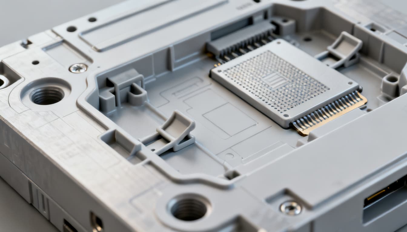
Designing Electronics Housings for Injection Molding: 7 Common Mistakes That Compromise EMI Shielding and Snap-Fit Integrity
In 2023, an automotive-tier supplier made a decision that seemed financially prudent on paper: substitute standard ABS for the specified glass-filled nylon (PA66-GF30) in an under-hood sensor housing. The material cost savings amounted to roughly $0.02 per snap-fit clip. Two months after vehicles hi
When a 2-Cent Clip Failure Grounds a Production Line: The Real Cost of Housing Design Oversights
In 2023, an automotive-tier supplier made a decision that seemed financially prudent on paper: substitute standard ABS for the specified glass-filled nylon (PA66-GF30) in an under-hood sensor housing. The material cost savings amounted to roughly $0.02 per snap-fit clip. Two months after vehicles hit the road, the clips began failing. Sustained heat exposure—routine for an engine-bay environment—had embrittled the ABS beyond its glass-transition tolerance. Snaps fractured during normal vibration, sensor housings separated, and a production line ground to a halt while engineers scrambled to contain the fallout [3].
That failure cascaded beyond mechanical retention. When snap-fits crack, housing halves lose compressive contact. Conductive gaskets unseat. EMI shielding gaps open. What began as a material substitution to shave pennies became a field-recall liability with six-figure containment costs.
Draft-related failures tell a parallel story. Consider a PA66+30% GF housing with a VDI-24 textured interior wall and a draft angle of just 1°. During ejection, the textured surface drags against the mold steel. The result: micro-tearing, stress whitening, and subsurface cracks that may not be visible at final inspection but propagate under thermal cycling [1]. If that housing carries a nickel-copper conductive coating—common for 40–60 dB shielding—those micro-cracks become discontinuities in the conductive path. The shield leaks. The product fails EMC compliance testing, and the root cause traces back to a draft angle that someone guessed instead of calculated.
Key Takeaway: Electronics housing failures are rarely single-point events. A draft angle error becomes an ejection defect, which becomes a coating discontinuity, which becomes an EMI leak. A material substitution becomes a snap-fit fracture, which becomes a gasket unseating, which becomes a shielding failure. The design decisions you make today on wall thickness, draft, and material selection are the failure-mode chain you'll debug in 18 months.
The Three Numbers That Define Every Electronics Housing: Wall Thickness, Draft, and Shrink
Before you place a single snap-fit or specify an EMI gasket groove, three interdependent parameters govern whether your housing will mold cleanly, eject without damage, and maintain dimensional stability through its service life. They are not independent variables—change one, and the other two shift.
Wall Thickness: The Foundation of Fill and Flatness
Molten plastic follows the path of least resistance. When wall thickness varies abruptly, flow fronts split, race ahead through thick sections, and reunite at unpredictable locations—creating weld lines exactly where you don't want them. Worse, thick sections cool more slowly than thin ones, generating differential shrinkage that manifests as sink marks. A sink mark as shallow as 0.05 mm is enough to create a gap under a conductive EMI gasket, and that gap is a slot antenna at GHz frequencies [6].
The table below summarizes recommended nominal wall thickness ranges for resins commonly specified in shielded electronics housings. These values balance moldability, structural stiffness, and cycle time.
| Resin | Nominal Wall Thickness (mm) | Max Rib Thickness (% of wall) | Typical Shrinkage (%) | Notes for EMI Housings |
|---|---|---|---|---|
| PC/ABS (unfilled) | 1.5–3.0 | 60% | 0.5–0.7 | Good balance of flow and impact; widely used for indoor electronics |
| PA66-GF30 | 1.5–3.0 | 50–60% | 0.3–0.5 | Higher stiffness; requires more draft on textured surfaces |
| PC (unfilled) | 1.5–3.0 | 60% | 0.5–0.7 | Excellent transparency option; higher melt viscosity |
| ABS (general purpose) | 1.2–2.5 | 60% | 0.4–0.6 | Cost-effective but limited thermal resistance; avoid for >60°C sustained |
| PC-CF (carbon-fiber filled, 10–20%) | 1.5–2.5 | 50% | 0.1–0.3 | Inherently conductive; reduced flowability; abrasive on tool steel |
| PA66-SSF (stainless-steel fiber, 6–10%) | 1.8–3.0 | 50% | 0.2–0.4 | Conductive throughout; heavier; requires hardened mold components |
Tip: When designing EMI gasket grooves, maintain the groove floor at the same nominal wall thickness as the surrounding housing. A thickened groove base may seem like a stiffness improvement, but it creates a sink-prone hot spot that defeats the flatness you're trying to achieve [7].
Draft: The Angle That Protects Your Conductive Coating
Draft is not a suggestion—it's a mechanical requirement dictated by the resin's shrink behavior, the surface texture depth, and the ejection stroke. For glass-filled nylons, the glass fibers orient along the flow direction and create micro-undercuts on textured surfaces. A draft angle of 1° on a VDI-24 texture is demonstrably insufficient; the industry data shows tearing and whitening at these parameters [1]. The minimum safe draft for light-textured PA66-GF30 is 1.5°–2° per side; heavy VDI textures demand 3°–5° [5].
Why does this matter for EMI? Because the conductive coating—whether electroless nickel-copper or vacuum-metallized aluminum—deposits onto the molded surface. If that surface is micro-cracked from ejection trauma, the coating inherits those discontinuities. You've built a shield with invisible seams.
Shrinkage: The Silent Geometry Shifter
Every thermoplastic shrinks as it cools from melt temperature to ambient. Glass-fiber fill reduces shrinkage (0.3–0.5% for PA66-GF30 vs. 1.0–1.5% for unfilled PA66), but it also introduces anisotropy—shrinkage differs parallel and perpendicular to flow. This means a snap-fit beam dimensioned at 2.00 mm in CAD may mold at 1.94 mm in the flow direction and 1.97 mm transverse to it. If your snap-fit deflection tolerance is ±0.05 mm, you've already consumed your margin before the part leaves the mold. Generous fillets at snap-fit roots and uniform wall stock throughout the housing help normalize shrinkage gradients [7] [8].
Where Snap-Fits Snap: The Seven Most Overlooked Design Details in Electronics Housings
Snap-fits are deceptively simple. A cantilever beam with a retention hook—what could go wrong? In electronics housings that must also provide EMI shielding, the answer is: quite a lot. The seven mistakes below are the ones that repeatedly surface in failure analysis reports, and each has a direct pathway to compromised shielding integrity.
| # | Mistake | EMI / Snap-Fit Consequence | Practical Fix |
|---|---|---|---|
| 1 | Insufficient draft on textured walls | Ejection micro-cracks break conductive coating continuity; shielding leaks at crack locations | Calculate draft mechanically: 1.5°–2° min for light texture, 3°–5° for heavy VDI [1] [5] |
| 2 | Non-uniform wall thickness | Sink marks at thick sections unseat EMI gaskets; 0.05 mm sink = measurable shielding gap | Maintain uniform 1.5–3.0 mm walls; ribs ≤60% of adjacent wall; use generous fillets [6] [7] |
| 3 | Material substitution without thermal-aging validation | ABS snaps embrittle and fracture under sustained heat; housing halves separate; gaskets unseat | Validate snap-fit material at maximum service temperature + 20°C margin; PA66-GF30 for >60°C applications [3] |
| 4 | Sharp internal corners at snap-fit roots | Stress concentration factor of 3–5× at sharp corners; fatigue cracks initiate within 100–500 cycles | Minimum fillet radius of 0.5 mm or 25% of beam thickness at every snap-fit root [7] [8] |
| 5 | Ignoring weld-line placement at snap-fit bases | Weld lines at snap-fit roots reduce flexural strength by 30–50%; snaps fracture on first assembly | Use mold-flow simulation to reposition gates; ensure weld lines fall away from snap-fit features [2] [4] |
| 6 | Misaligned PCB supports and connector cutouts | PCB standoffs preload snaps during assembly; constant stress accelerates creep and fatigue failure | Design boss height tolerance to match PCB standoff spec; allow 0.1–0.2 mm float in connector cutouts [9] |
| 7 | Omitting crush ribs for grounding contact | Intermittent electrical contact between housing halves; shielding effectiveness fluctuates with vibration | Add crush ribs (0.2–0.3 mm interference) along parting lines to maintain consistent grounding [7] |
Let's unpack a few of these in more detail, because the failure mechanisms are worth understanding at depth.
Mistake #3: The Material Substitution Trap
The automotive case from Section 1 is not an outlier—it's a pattern. ABS is an excellent general-purpose resin for indoor consumer electronics with low cycle counts and ambient temperatures. But its glass-transition temperature (Tg) hovers around 105°C, and sustained exposure above 60°C accelerates oxidative embrittlement. Snap-fits in ABS under constant deflection will creep, lose retention force, and eventually fracture. For any electronics housing that must survive more than 1,000 mating cycles or operate in environments exceeding 60°C, PA66-GF30 or a PC/ABS blend with appropriate heat stabilization is the defensible choice [3].
Mistake #5: Weld Lines at the Worst Possible Location
When two melt fronts meet, they don't fully intermix. The resulting weld line is a plane of reduced molecular entanglement—and reduced mechanical strength. In glass-filled resins, the fibers at a weld line orient parallel to the interface rather than across it, further degrading load transfer. If a weld line forms at the base of a snap-fit beam, the beam's effective flexural strength may be only 50–70% of the bulk material value [2]. Mold-flow simulation is not optional when snap-fit locations are constrained by housing geometry; gate placement must be optimized to push weld lines into low-stress regions [4].
Mistake #7: The Missing Ground Path
An EMI shield is only as good as its electrical continuity. When two conductive housing halves mate, the parting line is a potential slot radiator. Crush ribs—small raised features that deform plastically on assembly—create a continuous line of interference fit that bridges the gap. Without them, you're relying on the flatness of two injection-molded surfaces to maintain contact, and that flatness degrades with every thermal cycle. Specify crush ribs with 0.2–0.3 mm of interference, spaced no more than 25–30 mm apart along the parting line [7].
Conductive Plastics vs. Coated Housings: What Really Shuts Out EMI Without Breaking Snap-Fits
There are three dominant strategies for achieving 40–60 dB of shielding in injection-molded electronics housings, and each interacts differently with snap-fit design. The choice affects not just shielding performance but also tooling cost, snap-fit fatigue life, and long-term reliability.
| Comparison Metric | Nickel-Copper Coated PA66-GF30 | Carbon-Fiber-Filled PC (PC-CF, 15–20%) | Stainless-Steel Fiber PA66 (PA66-SSF, 6–10%) | Selection Criteria & Failure Boundary |
|---|---|---|---|---|
| Typical shielding effectiveness | 45–65 dB (1–10 GHz) | 30–50 dB (resistive, frequency-dependent) | 40–55 dB (broadband) | Coated PA66-GF30 for >50 dB requirements; PC-CF adequate for 30–40 dB consumer applications |
| Snap-fit fatigue life | High—base resin governs; coating adds negligible thickness | Moderate—carbon fibers reduce ductility; snaps may fail brittle at high deflection | Moderate—SS fibers create stress risers; fatigue life 20–30% lower than unfilled | Coated PA66-GF30 best for high-cycle (>1,000) snap applications; validate SSF snaps at max deflection |
| Coating adhesion after snap cycling | Requires validation; plating can delaminate at snap engagement surfaces after 100+ cycles | Not applicable—conductivity is bulk property | Not applicable—conductivity is bulk property | For coated housings, design snap engagement so coating isn't scraped; use crush ribs at parting lines [7] |
| Per-part cost (relative) | Medium—molding + secondary plating operation | Medium-high—higher resin cost, no secondary op | High—premium compound, abrasive on tooling | Coated PA66-GF30 often lowest total cost at volume; PC-CF eliminates plating logistics |
| Moldability / flow characteristics | Excellent—GF30 flows well in thin walls | Reduced—carbon fiber increases viscosity; minimum wall 1.8 mm recommended | Reduced—SS fibers increase viscosity; requires wider gates and higher injection pressure | PC-CF and PA66-SSF demand more generous gate dimensions and may limit minimum wall thickness [6] |
| Long-term conductivity retention | Dependent on coating integrity; corrosion at exposed edges possible | Stable—conductivity is inherent; no delamination risk | Stable—conductivity is inherent; slight oxidation possible at fiber ends | For outdoor or high-humidity applications, bulk-conductive compounds eliminate coating failure risk [8] |
The trade-off crystallizes around two questions: How many snap-fit cycles must the housing survive, and what is the acceptable shielding variance over the product's lifetime? Coated PA66-GF30 offers the best snap-fit fatigue performance because the base resin's mechanical properties are well-characterized and the coating is microns thick. But if the coating delaminates at snap engagement points after repeated mating—a failure mode observed in field returns—shielding degrades unpredictably. Bulk-conductive compounds like PC-CF and PA66-SSF eliminate the coating variable entirely, at the cost of reduced snap-fit ductility and higher material pricing [8].
Note: If you choose the coating route, design the snap-fit engagement surfaces so that the coating is not the primary wear surface. A small relief (0.05–0.1 mm) on the snap hook's contact face, combined with crush ribs at the parting line, preserves coating continuity where it matters most—at the shielding envelope [7].
Snap-Fit and EMI Shielding Design Questions Engineers Ask Before Cutting Steel
After hundreds of mold-design reviews and failure analyses, certain questions surface repeatedly. Here are the five that senior engineers and procurement leads ask most often—with answers grounded in real defect data and production experience.
Q: What draft angle is really needed for a VDI-textured PA66+30% GF housing to avoid stress cracking?
A minimum of 1.5°–2° per side is recommended for light textures (VDI 12–18). For heavier textures (VDI 24 and above), increase to 3°–5° per side. The common mistake of specifying 1° draft—often carried over from unfilled resin experience—leads to ejection tearing and whitening. In glass-filled PA66, the fibers create microscopic undercuts against textured steel; insufficient draft means those fibers are literally ripped from the surface during ejection. The resulting micro-cracks, even if visually subtle, break the continuity of plated EMI shields and create initiation sites for fatigue cracks under thermal cycling [1] [5].
Q: Can I use standard ABS for indoor electronics housings with snap-fits, or will it fatigue?
ABS can work for low-cycle (under 100 matings), room-temperature indoor applications where the snap-fit is not under sustained deflection. However, ABS is prone to creep under constant load and becomes brittle with age, particularly if exposed to any heat source—including the waste heat from enclosed PCBs. For snap-fits that must survive 1,000+ assembly cycles or operate in environments exceeding 60°C, glass-filled nylon (PA66-GF30) or heat-stabilized PC/ABS blends are far more reliable. The automotive case study where ABS clips snapped after two months of under-hood heat exposure is a documented cautionary tale [3].
Q: How do I maintain 40 dB shielding when using a conductive coating on a snap-fit enclosure?
Three design rules: First, ensure the coating is applied after all snap features are molded—never machine or modify snaps post-coating. Second, design snap-fit engagement so that the coating is not scraped off during repeated assembly; a small relief (0.05–0.1 mm) on the snap hook's contact face prevents metal-on-metal abrasion of the coating. Third, use crush ribs or conductive gaskets at parting lines to bridge any coating discontinuities that develop over time. Validate adhesion after a minimum of 100 mating cycles using tape-test methods per the coating supplier's specification [7] [6].
Q: What wall thickness range prevents sink marks that can unseat EMI gaskets?
Keep nominal walls between 1.5 and 3.0 mm for electronics-grade resins, and avoid sudden transitions—gradual tapers of 3:1 or gentler are preferred. Ribs should be no more than 60% of the adjacent wall thickness. A sink mark as shallow as 0.05 mm creates a measurable gap under a conductive gasket; at frequencies above 1 GHz, that gap behaves as a slot antenna. Use uniform wall stock throughout the housing and generous fillets (minimum 0.5 mm radius) at all internal corners to normalize cooling rates and ensure flat sealing surfaces [6] [7].
Q: What is the most overlooked DFM check for PCB mounting bosses in molded housings?
Boss design is the most common source of sink marks on the opposite housing face—and it's almost always because the boss base is too thick. The boss outer diameter should be approximately 2× the screw diameter, with a wall thickness around 0.8× the nominal housing wall. A minimum 0.5° draft on the boss ID and OD is essential for clean ejection. Critically, the boss height tolerance must align with the PCB standoff specification; a boss that is 0.2 mm too tall preloads the snap-fits during PCB assembly, placing them under constant stress that accelerates creep and fatigue failure. Verify the entire tolerance stack—boss height, PCB thickness, standoff height, and screw head clearance—before cutting steel [9] [1].
Designing electronics housings that maintain both mechanical integrity and EMI shielding performance is a systems problem. The snap-fit that retains your housing is also part of your grounding path. The wall thickness that determines your cycle time also determines whether your gasket seats flat. The draft angle that seems like a minor detail on a drawing is what preserves—or destroys—your conductive coating. Every parameter connects. The seven mistakes outlined here are not theoretical; they are drawn from production failures, field returns, and the hard-won experience of engineers who've debugged them at scale. If you're preparing a housing design for tooling, invest the time in mold-flow simulation, validate your material choice at temperature, and never guess on draft. The cost of getting it wrong is measured in recalls, not rework.
Ready to review your electronics housing design with a team that understands both injection molding and EMI shielding requirements? Contact PandaMolding for a DFM consultation before you cut steel.
References & Further Reading
- a